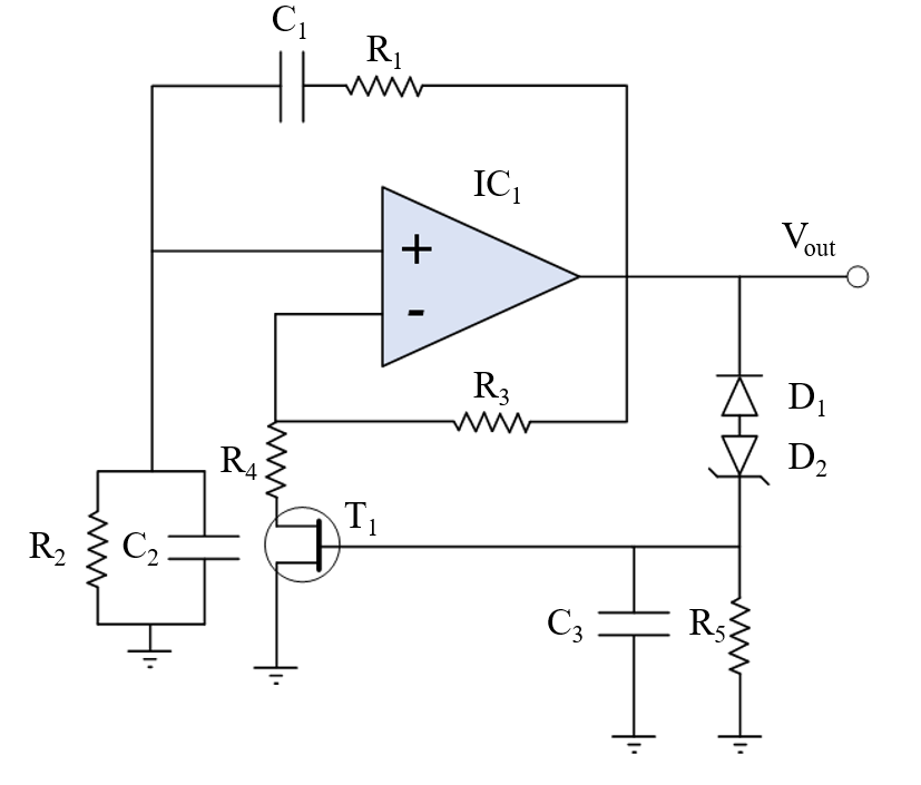
Wien Oscillation Circuit
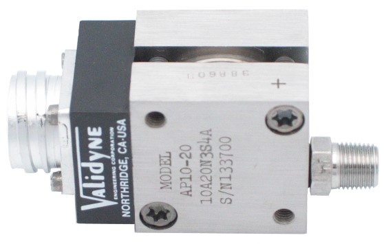
To support the use of AP10 valydine pressure sensor in cryogenics, design was needed to generate 5 kHz sinusoidal waveform with ±5V peak-to-peak output. The design is specified to function in radiated environments.
The Wien-bridge oscillator is a widely used configuration for generating low-frequency sine waves. It is favoured for its simplicity, stability, and minimal dependency on the specific characteristics of the operational amplifier used in the circuit. The oscillator operates based on the principle of a resistive-capacitive (RC) network, which determines the oscillation frequency.
• The total phase shift around the loop must be zero (or an integer multiple of 2π).
• The loop gain must be exactly unity.
The Wien-bridge network consists of two RC pairs:
• R1 and C1 introduce a phase shift in the signal.
• R2 and C2 provide an opposing phase shift.
At a specific frequency, these phase shifts cancel out, ensuring that the net phase shift is zero. Additionally, the gain of the amplifier stage must be precisely three to counteract the attenuation introduced by the Wien-bridge network. Wien Bridge Oscillator equations are:
1. Frequency of Oscillation:
\[ f = \frac{1}{2\pi R_4 C_1} = \frac{1}{2\pi R_2 C_2} \]
This equation determines the oscillation frequency based on the resistor and capacitor values in the circuit.
2. Series Impedance (Zs):
\[ Z_s = \sqrt{R_1^2 + \frac{1}{(2\pi f C_1)^2}} \]
This represents the impedance of the series combination of the resistor and capacitor.
3. Parallel Impedance (Zp):
\[ Z_p = \sqrt{\left(\frac{1}{R_2}\right)^2 + (2\pi f C_2)^2} \]
This is the impedance of the parallel resistor and capacitor network.
4. Voltage Relationship:
\[ V_2 = \frac{V_{out}}{1 + \frac{Z_p}{Z_s}} \]
If \( R_1 = R_2 \) and \( C_1 = C_2 \), then:
\[ V_2 = \frac{V_{out}}{3} \]
This means the voltage at that node is one-third of the output voltage.
5. Gain of the Oscillator:
\[ \text{Gain} = \frac{2Z_p + Z_s}{Z_p} \]
This equation describes the gain required to sustain oscillations in the circuit.
6. Alternative Gain Expression:
\[ \text{Gain} = 1 + \frac{R_3}{R_4 + R_{DS}} \]
This is another form of the gain equation, incorporating resistors that help control the oscillation conditions.
Despite its theoretical simplicity, practical implementation of the Wien-bridge oscillator presents several challenges:
- Component tolerances: Resistors can be manufactured with tight tolerances, but capacitors often exhibit significant variability. This affects both the oscillation frequency and gain stability.
- Gain stability: If the amplifier gain is insufficient, oscillations will not start; if excessive, the output waveform becomes distorted.
- Manual gain control: Traditional implementations require a variable resistor in the feedback path to fine-tune the gain, which increases complexity and introduces manufacturing inefficiencies.
To address these issues, a Junction Field-Effect Transistor (JFET) can be introduced into the feedback loop to regulate the gain dynamically. This method eliminates the need for manual adjustments and enhances the circuit’s stability.
Operating Principle of the JFET in the Wien-Bridge Oscillator:
• At startup, the JFET's gate voltage is zero, resulting in a low drain-source resistance. This increases the amplifier gain beyond the required threshold, ensuring that oscillations begin.•As the oscillations develop, the negative half-cycles of the output signal are rectified and applied as a control voltage to the JFET gate. This increases the JFET’s resistance, reducing the amplifier gain and stabilizing the oscillation amplitude.
•The circuit self-adjusts, maintaining oscillations without excessive distortion or over-amplification.
The integration of a JFET for automatic gain control provides several key advantages:
- Elimination of Manual Adjustments: The circuit can achieve and maintain stable oscillations without requiring precise tuning of resistors.
- Consistent Amplitude Control: The JFET dynamically regulates the gain, ensuring a stable output signal with minimal distortion.
- Improved Reliability: The circuit automatically compensates for component tolerances, making it more robust in practical applications.
A JFET (Junction Field-Effect Transistor) is a voltage-controlled semiconductor device that regulates current flow between the drain and source using an electric field. It has high input impedance and is commonly used in amplifiers, oscillators, and signal processing circuits.
For small drain-to-source voltages (VDS) around zero (e.g., ±25 mV), a JFET exhibits nearly symmetric resistance for positive and negative VDS. This means that whether VDS is slightly positive or slightly negative, the drain-to-source resistance (RDS) remains approximately the same. This behaviour occurs because, in the ohmic region, the JFET channel acts as a resistive element controlled by the gate-to-source voltage (VGS). Since the channel remains unsaturated at low VDS, current flow follows a nearly linear relationship, and the JFET functions similarly to a voltage-controlled resistor. While the resistance does change with VDS, the variation is minimal for small signals, making the JFET suitable for low-distortion applications such as amplitude stabilization in Wien-bridge oscillators.
At the beginning of the design phase, multiple JFETs were tested to evaluate how consistently their resistance remained for both positive and negative low VDS values. Among the tested devices, the 2N3819 exhibited the best performance, showing the most symmetrical resistance behaviour in this region. The goal was to select a steady-state operating point where RDS would be as high as possible. This approach minimizes the impact of resistor tolerances on circuit performance. However, increasing VGS (which results in a higher RDS) also leads to greater asymmetry between the positive and negative RDS values. Therefore, a compromise was necessary.
For this application, a VGS of -2.3V was chosen, as the 2N3819 provides a resistance of approximately 1 kOhm at this point. The operating point was set to ±25 mV with respect to VDS. Test results for the 2N3819 are shown in the following table.
| Vgs (V) | Vds = ±25mV | Vds = ±50mV | ||||
|---|---|---|---|---|---|---|
| Rds Positive (Ω) | Rds Negative (Ω) | Deviation (%) | Rds Positive (Ω) | Rds Negative (Ω) | Deviation (%) | |
| 0 | 158 | 156 | 0.64% | 158 | 155 | 0.96% |
| -0.1 | 247 | 242 | 1.02% | 248 | 241 | 1.43% |
| -0.25 | 276 | 271 | 0.91% | 278 | 267 | 2.02% |
| -0.5 | 314 | 307 | 1.13% | 316 | 305 | 1.77% |
| -0.75 | 366 | 357 | 1.24% | 369 | 353 | 2.22% |
| -1.0 | 442 | 427 | 1.73% | 446 | 422 | 2.76% |
| -1.25 | 565 | 554 | 2.17% | 574 | 532 | 3.8% |
| -1.5 | 663 | 629 | 2.63% | 676 | 618 | 4.48% |
| -1.75 | 811 | 759 | 3.31% | 832 | 744 | 5.79% |
| -2.0 | 1058 | 966 | 4.55% | 1093 | 935 | 7.79% |
| -2.25 | 1533 | 1350 | 6.35% | 1603 | 1288 | 10.9% |
| -2.5 | 2618 | 2170 | 9.36% | 2789 | 2027 | 15.82% |
| Component | Value/Description | Part number(s) |
|---|---|---|
| R1 | 127K 0.1% | 603-RT0805BRD07127KL |
| R2 | 12K7 0.1% | RN73C2A12K7BTDF |
| R3 | 200K 0.1% | 754-RG2012P-204-B-T5 |
| R4 | 9K9 0.1% | 603-RT0805BRD079K09L |
| R5 | 5K2 0.1% | RT0805BRD072K2L & ERA6ARB302V |
| C1 | 250 pF | 581-12061A251FAT2A |
| C2 | 2500 pF | 581-12061A152FAT2A & 581-12061A102F |
| C3 | 10 uF | C1206C106K3PACTU |
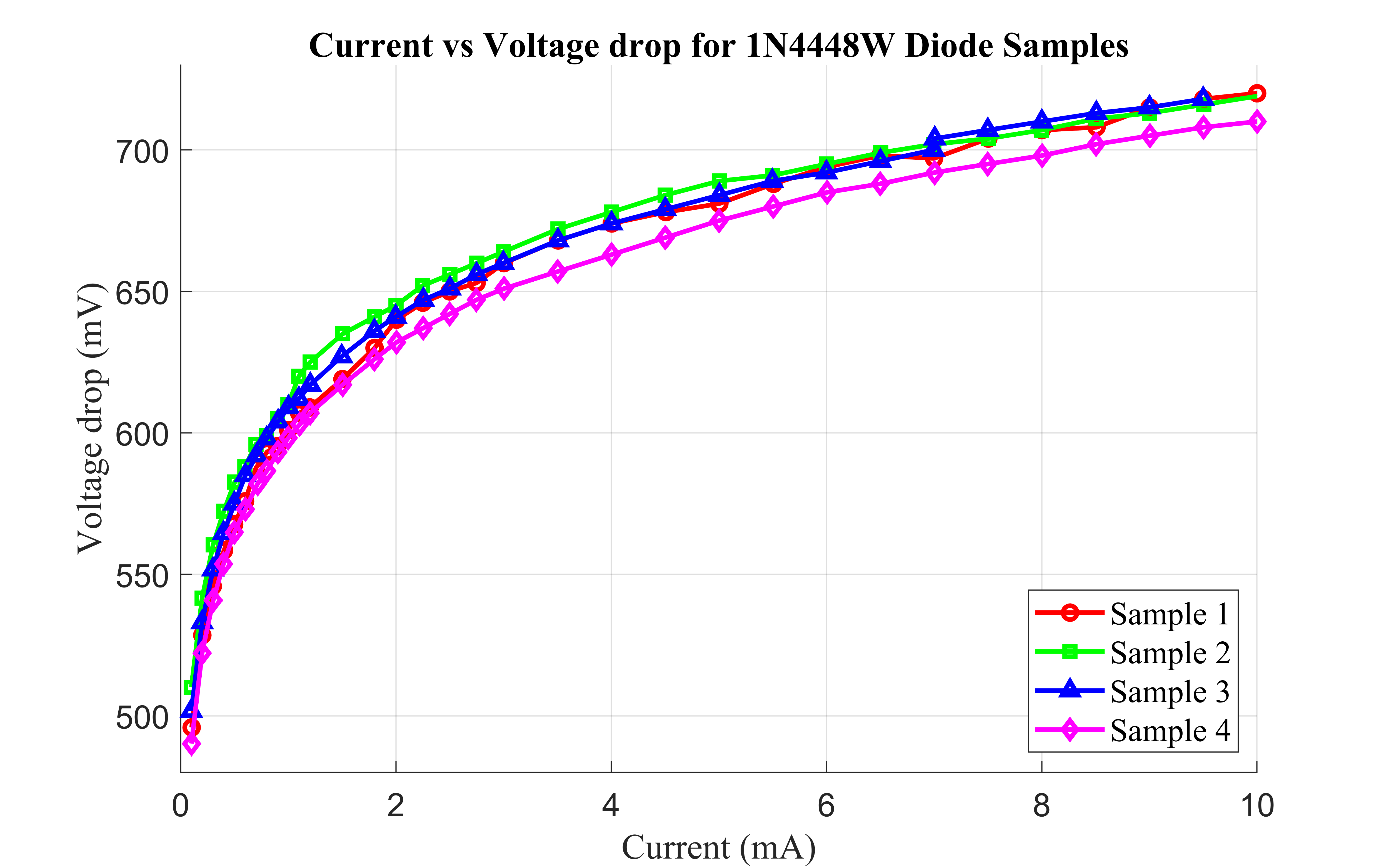
| D1 | Fast switching diode | 1N4448W |
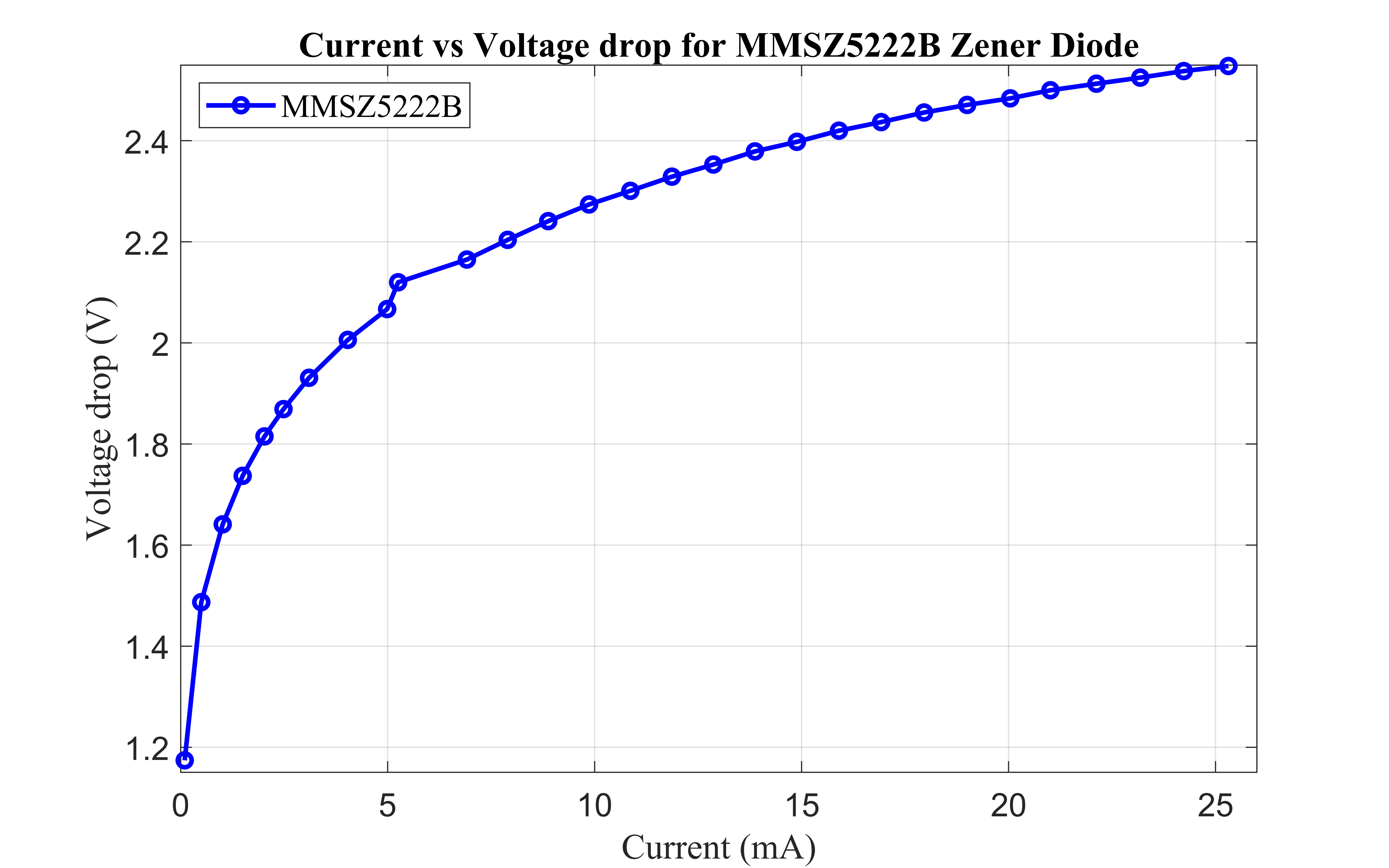
| D2 | Zener diode | MMSZ5222 |
| IC1 | Operational Amplifier | OPA602AU |
| T1 | JFET | 2N3819 |
The selected JFET operating point was:
• RDS ≈ 1 Kohm
• VDS ≈ ±25mV
• IDS ≈24 μA
A gain of 21 was used in the design. For the feedback path, precise diode selection was critical, requiring a combination of a Zener diode and a 1N4448 diode. Since the voltage drop across a diode varies with current, laboratory testing was conducted to optimize circuit performance. These tests involved measuring the voltage drop across the 1N4448W diode under different current levels. Similarly, the MMSZ5222B Zener diode, which has a rated voltage drop of 2.3V at 20mA as per the datasheet, was also characterized to ensure stable circuit operation.
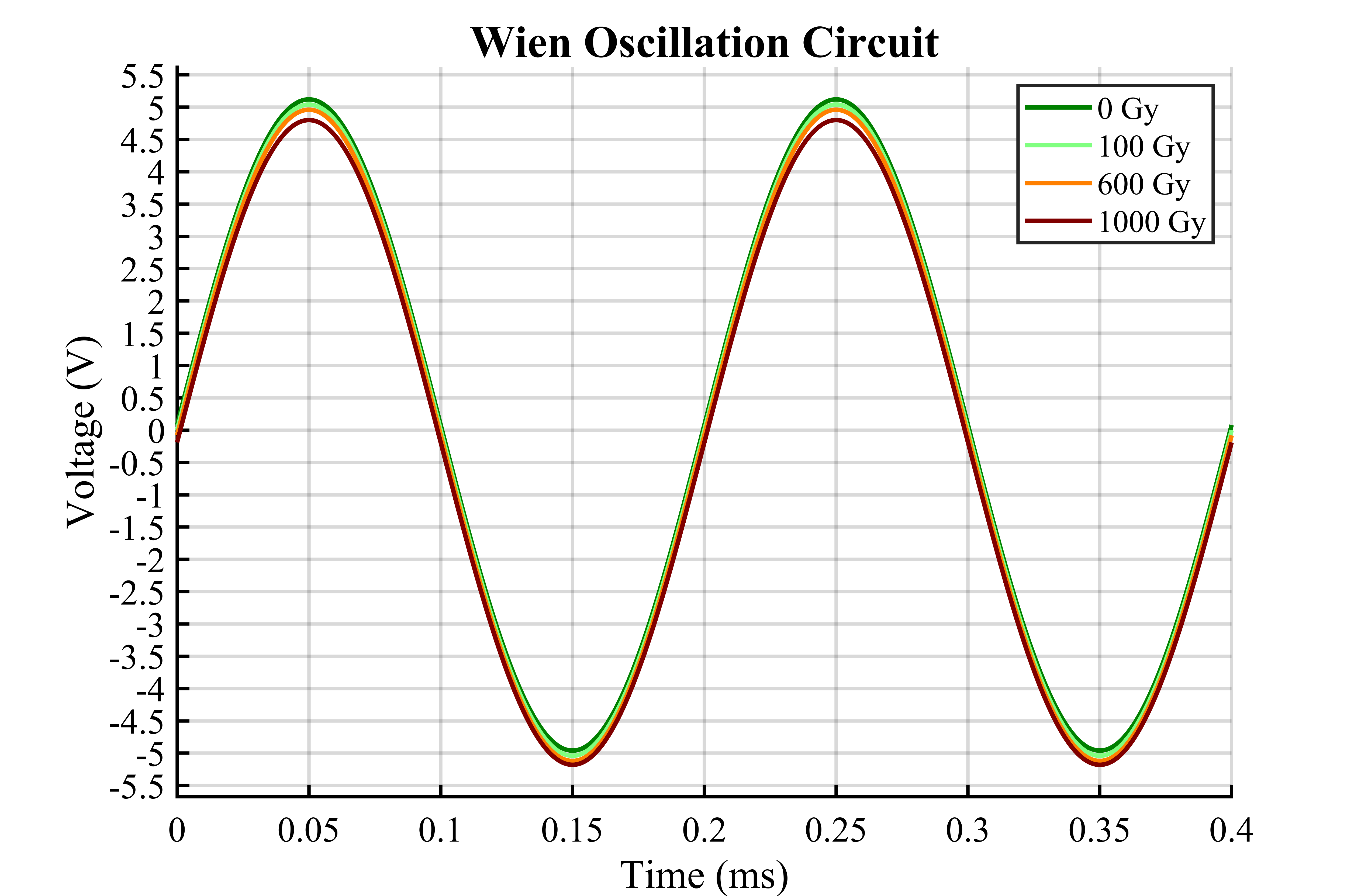
| 0 Gy | 100 Gy | 600 Gy | 1000 Gy | |
|---|---|---|---|---|
| Positive peak (V) | 5.12 | 5.04 | 4.96 | 4.8 |
| Negative peak (V) | -4.96 | -5.04 | -5.12 | -5.18 |