New Communication Card
System Architecture
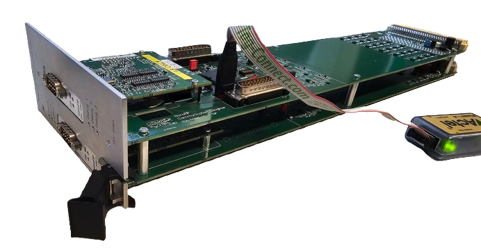
The cryogenics crate houses several types of electronics required for system operation, including peripheral cards that collect measurements from temperature sensors, power cards that supply the crate electronics, and communication cards that exchange data between the peripheral cards and the WorldFIP network.More than 1000 communication cards are currently deployed, primarily across the Large Hadron Collider (LHC). Each communication card acts as a WorldFIP node and consists of a motherboard and daughterboard, with each board connected to its own FPGA Mezzanine Card (FMC). The motherboard collects data from the peripheral cards on the left side of the crate, while the daughterboard handles the cards on the right side. Each board contains an FPGA responsible for processing and transferring its corresponding peripheral-card data.

As additional cryogenic crates were required for future LHC infrastructure, the existing MicroFIP-based design could not simply be reproduced: the obsolete MicroFIP and the new NanoFIP solutions were not one-to-one replacements. This required a new communication-card architecture based on the NanoFIP FMC while maintaining compatibility with the existing WorldFIP infrastructure.

Hardware & FPGA Design
I owned the hardware and FPGA development of the new motherboard and daughterboard, taking the design through development, validation, qualification, and production.

Peripheral crate cards → FPGA → Wishbone → NanoFIP FMC → WorldFIP
The FSM controls the required read and write operations, providing the hardware interface between the peripheral-card data and the WorldFIP communication layer.
Solving the 120-Byte WorldFIP Payload Constraint
The WorldFIP network imposes a strict 120-byte payload limit per node. In the existing architecture, the motherboard handled more peripheral channels than the daughterboard, leaving one motherboard-side channel unused because the available payload allocation was already fully utilized.Rather than carrying this limitation into the new design, I identified an opportunity to use the unused capacity on the daughterboard. I implemented a dedicated I2C link between the motherboard and daughterboard FPGAs, allowing the motherboard FPGA to transfer the excess 8 bytes to the daughterboard for transmission through its available WorldFIP payload capacity.
This improvement enabled the new communication card to use all crate channels and transmit the complete set of available data from the left side of the crate, while remaining within the WorldFIP payload constraint.

Validation & Production
I led the laboratory validation of the complete communication card, testing the hardware in a cryogenic test crate populated with the relevant peripheral cards. The system was exercised under representative operating conditions while crate data was continuously captured and documented for analysis.I developed Python-based analysis scripts to process the recorded data and automatically detect communication errors, providing an automated check of data integrity across extended test runs.
At the hardware level, I used oscilloscope measurements to verify the physical Wishbone signals, including signal integrity, clock quality, and setup/hold timing. FPGA integrated logic-analysis tools were used to inspect internal state-machine operation and data transfers.
I also led the CHARM 2024 radiation campaign, coordinating the radiation testing and evaluating the communication card under the expected radiation environment.
Following successful validation and qualification, I owned the transition of the communication card into production, with 400 units produced for CERN's cryogenic control infrastructure.